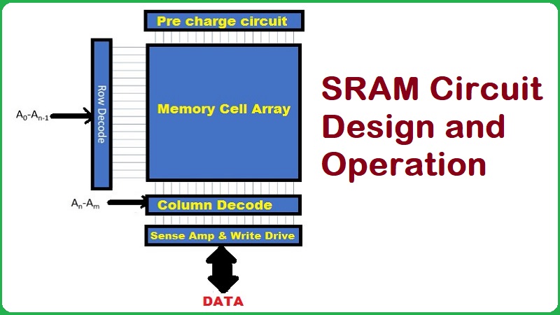
Hello Friends! Today, through this article we are going to show you all possible things about SRAM circuit design and operation (read/write); as well as how does it work? Let’s start!!
SRAM is totally different to DRAM because DRAM requires regularly refreshing data that is store in the memory. So, SRAM’s speed is fastest to DRAM as well as it consume less power to DRAM.
In SRAM, All data has been stored in flip-flop. Flip-flop contains the every bit of this Ram. Flip-flop uses 4-6 transistors for making a memory cell and its circuit do not need to refreshment continuously. SRAM helps to store every bit with using of bitable latching circuitry, and typically it used six MOSFET to store every memory bit but extra transistor become at smaller nodes.

SRAM holds a bit of data on 4 transistors with using of 2 cross coupled inverters, and it has two stable states like as 0 and 1. Due to read and write operations, other two access transistors are using to handle the availability for memory cell.
It needs 6 MOFSET (metal-oxide-semiconductor field-effect transistor) to hold per memory bit. MOFSET is also one type of SRAM chip, and other is bipolar junction transistor. Bipolar junction transistor’s speed is fastest but it uses much power.
SRAM Circuit Design and Operation
Static Random Access Memory cell designed with two inverters that cross-linked like as latch form. This latch made connection to two bit line along with two transistors T1 and T2.
Also Read: What is RAM? Types, Uses and Functions with Examples!
Now both transistors are capable to alter their modes (open or close) under control of word line, and this entire process is getting control by address decoder.
When word line goes to ground level then both transistors get turned off, and latch starts to retain own state.

How Does Work Static RAM?
Static RAM working get divide into three operations like as Read, Write and Hold.
Read Operation
Both switches T1 and T2 are closed while activating the word line. When, cell comes to state 1 then signal flows in high amount on b line and other side signal flows in low amount on b’ line. Opposite is true when cell goes to state 0. Finally both b and b’ get complement of each other’s.
Sense/write, which connected in the rear side of two bit line, they monitor their states and finally convert into output respectively.
Write Operation
In the write operation, Sense/Write circuit allows to drive bit lines b and it complement b’, and then it provides accurate values on bit line b and b’ as well as go to activate word line.
Hold Operation
For Hold Operation both access transistors must be turn OFF (T1 and T2). Due to presence of latching element SRAM hold its state.
Main objective of using the static RAM is to make Cache Memory. Static Ram is more expensive; because it made with using of much complicated structure. But, its complexity is also limited for storing amount of data into one chip. Due to this, SRAM chips have not ability to hold much data compare to DRAM.
So, SRAM is also using mostly in to small size applications like as CPU cache memory and hard drive buffers, compact discs (CD’s), printers, modem, routers, digital versatile discs (DVD’s) and digital cameras.


